
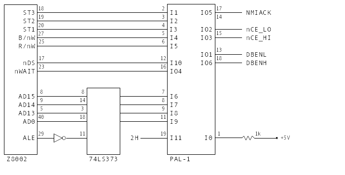
There are two Z8002 CPUs in Pole Position, labelled A and B. Each has a custom logic chip labelled PAL-1. Here is a portion of the schematic redrawn.
Chip Analysis
It's evident from the analysis that PAL-1 decodes certain Z8002 bus transactions, and generate signals to complete those transactions.
Silicon
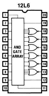
Atari indicates PAL-1 is simply a a programmed PAL 12L6. These 1980s-era PALs have 12 inputs and 6 outputs. Each output is an inverted sum-of-products of the inputs.
Testing
A sample of PAL-1 was wired into a circuit where the 12 inputs were connected to a serial-to-parallel shift register, and the 6 outputs connected to a parallel-to-serial shift register. An MCU coordinated the application of test patterns and the capture of the output state.
A linear-feedback shift register was implemented in the MCU firmware to generate all possible input test patterns. This was selected for efficiency since each subsequent test pattern only requires a single bit to be clocked to the stimulus shift register.
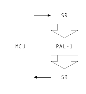
All six outputs were captured for For each test pattern. Comparing all combinations generated a truth table with 4096 entries. This truth table was analyzed with a simple Python program to generate the logic equations for each PAL-1 output.
Results
The tests develop the boolean expressions for each output as a function of inputs.
It is evident that none of the outputs depend on on the ST2 signal present at pin 3. Perhaps this signal was added early in the Pole Position design process, and not removed when detailed design revealed it as unnecessary.
NMIACK
NMIACK = /(ST3·/BAD15·/RnW·/ST1·BAD13·BAD14·/nDS)
So NMIACK asserts (low) when:
ST[3:0] = 1x0x (data request, stack request, or instruction fetch),RnW = 0 (write),nDS = 0 (data strobe), andADDR = 011x xxxx xxxx xxxx
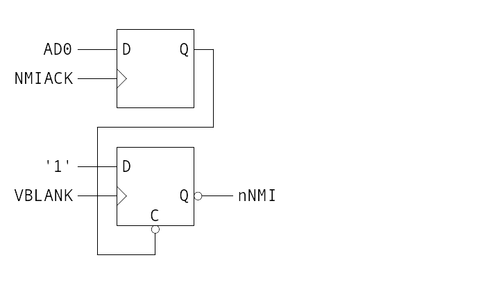
This generates a pulse can change the state of the latching non maskable interrupt to the CPU. The NMI is normally asserted by latching the VBLANK signal rising edge. When the NMIACK pulse occurs, and the LSB of the data bus (AD0) is zero, the NMI latch is asynchronously cleared. The NMI will not fire again until after the NMIACK pulse occurs with AD0=1, which re-enables the VBLANK latch. So long as the last value written to the NMIACK has AD0=1, the NMI will trigger on the next rising edge of VBLANK.
Chip Selects
nCE_LO = /(ST3·/BAD15·RnW·/ST1·/BAD14)
nCE_HI = /(ST3·/BAD15·RnW·/ST1·BAD14)
So these CE signals assert when:
ST[3:0] = 1x0x (data request, stack request, or instruction fetch),RnW = 1 (read), andADDR = 0Axx xxxx xxxx xxxx
These are the low-bank/high-bank chip selects for the ROMs connected to the CPU. The _LO signal asserts when reading addresses 0x0000-0x3fff. The _HI signal asserts when reading addresses 0x4000-0x7fff.
Data Bus Lanes
DBENL = /((ST3·/BnW·BAD15·/ST1) + (ST3·BnW·BAD15·/ST1·BAD0))
DBENH = /((ST3·/BnW·BAD15·/ST1) + (ST3·BnW·BAD15·/ST1·/BAD0))
Both of these data bus lane enables assert when:
ST[3:0] = 1x0x (data request, stack request, or instruction fetch),BnW = 0 (word access), andADDR = 1xxx xxxx xxxx xxxx
The low-order lane enable also asserts when:
ST[3:0] = 1x0x (data request, stack request, or instruction fetch),BnW = 1 (byte access), andADDR = 1xxx xxxx xxxx xxx1 (odd addresses)
The high-order lane enable also asserts when:
ST[3:0] = 1x0x (data request, stack request, or instruction fetch),BnW = 1 (byte access), andADDR = 1xxx xxxx xxxx xxx0 (even addresses)
This reveals that the 16-bit external bus is mapped read-write into addresses 0x8000-0xffff, both byte and word accesses are allowed. Byte accesses at odd addresses are "low", and even addresses are "high". This is consistent with the Z8002 being a big endian implementation.
nWAIT
nWAIT = /(ST3·BAD15·/ST1·2H)
So nWAIT asserts when:
ST[3:0] = 1x0x (data request, stack request, or instruction fetch),2H = 1 (horizontal scan pixel mod 4 is 2 or 3), andADDR = 1xxx xxxx xxxx xxxx
This prevents the Z8002 CPU from performing transactions on the external bus (e.g. screen memory), by inserting wait states. Presumably this is designed so the video hardware may have unfettered access to screen memory while rastering out pixels.
Summary
PAL-1 determines the memory map of the two Z8002 CPUs.
| Address Range | Word Read | Word Write | Byte Read | Byte Write |
|---|---|---|---|---|
0x0000 to 0x3fff |
Low ROMs | Low ROMs | ||
0x4000 to 0x7fff |
High ROMs | High ROMs | ||
0x6000 to 0x7fff |
NMIACK |
NMIACK |
||
0x8000 to 0xffff |
DBENL, DBENH |
DBENL, DBENH |
DBENL/H (odd/even) |
DBENL/H (odd/even) |